2012年11月28日 星期三

Mini-project: Sokoban


               On these two weeks, we need to do the mini-project. The project title is Sokoban. That means we need to write a assembly game of Sokoban. In this game,  Player pushes boxes or crates around in a warehouse, trying to get them to storage locations.
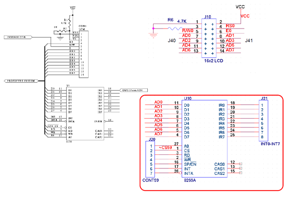
              First of all, we need to connect the graphical LCD (128X64) and 6X4 keypad to our system board.

Schematic of keypad
pin assignment of graphic LCD


Here is the result of our final circuit


Final product


             And we write a test program to test whether the LCD display is work correctly or not. And finally we found out it is work. In this wrap wire experience, I feel some trouble on testing the circuit is work or not. However, I have learnt how to use CRO to find out the problem. I use CRO to trace the signal. Finally, I found out a active low pin remains low at all time. This technique is very useful.
           Now, we still are writing our assembly game. This is a challenging project. The workload is a bit high. We have to finish this project within 3 weeks. Therefore, we need to take the extra session to do this project. Although, this project is tough, I have learnt more things from this course. 


Experiment 6 -- Interface of the 8088 MPU with the 8259A PIC and LCD Module


In this week, I have done the experiment 6. This lab is to study the interfacing of the 8259A PIC with the 8088 MPU and the interfacing of the LCD module with the 8088 MPU. I need to Wrap wire the control signals of the 8259A and LCD module as shown in the lab manual, modify the I/O address field of the given test program to match our design of address decoder. Finally I need to write my own program to fulfill the following function, the switch button is pressed, my name and ID will display on the LCD.  When the button is pressed again, my partner’s name and ID will display on the LCD.


I need to according to the above figure to wrap wire, The typical one is pin7-14 of Character LCD are connected to AD0~AD7.  The pin 6 of character LCD is connected to GAL  pin17 which I have modified the address decoder  for selecting the character LCD.

For writing this assembly program, I need to initialize all the devices first. I write to loop function which can display the name of my partner and I sequentially.
     
loop1:
check2: call check_key1
        jnc check2
        mov      dx,lcd_base
        call TURN_LED1_ON
        call display1
        mov cx,50
        call delay_X
       
check: call check_key1
        jnc check
        mov      dx,lcd_base

        call TURN_LED2_ON    
        call display2 
        mov cx,50
        call delay_X           
jmp loop1

Also I have to write the display string function, which can display name on the LCD display.
        outs1 db 'Cheng Ka Kui',0dh
        outs2 db '1155003893',0dh
        outs3 db 'Tai Pit Tat',0dh
        outs4 db '1155023064',0dh            
                       
display1   PROC      NEAR
        mov      dx,lcd_base
busy7:     in         al,dx
        and       al,10000000b
        jnz        busy7
        mov      al,00000001b    ;clear screen
        out        dx,al
;display string1
        mov      dx,lcd_base
busy10:   in         al,dx
        and       al,10000000b
        jnz        busy10
        mov      al,10000000b    ;set display address to 0
        out        dx,al
        mov      bx, offset outs1
        call        print_string
;display string2               
        mov      dx,lcd_base
busy20:   in         al,dx
        and       al,10000000b
        jnz        busy20
        mov      al,11000000b    ;set display address to 0
        out        dx,al
        mov      bx, offset outs2
        call        print_string
        ret
display1   ENDP

display2   PROC      NEAR
        mov      dx,lcd_base
busy72:   in         al,dx
        and       al,10000000b
        jnz        busy72
        mov      al,00000001b    ;clear screen
        out        dx,al
;display string3
        mov      dx,lcd_base
busy12:   in         al,dx
        and       al,10000000b
        jnz        busy12
        mov      al,10000000b    ;set display address to 0
        out        dx,al
        mov      bx, offset outs3
        call        print_string
;display string4               
        mov      dx,lcd_base
busy22:   in         al,dx
        and       al,10000000b
        jnz        busy22
        mov      al,11000000b    ;set display address to 0
        out        dx,al
        mov      bx, offset outs4
        call        print_string
        ret
display2   ENDP

Here is the result of our lab.


              After doing this lab, I have learnt how to write the assembly program. This is a very interesting lab. I can wrap wire to connect the device and write our own program. When the LCD can display the name and ID successfully, we felt a great sense of achievement.

2012年11月7日 星期三

Experiment 5 -- Parallel I/O and Timer/Count Interface


        On this two week, I had done the lab 5. The objective of Lab 5 is to study the interfacing of the 8255 PPI and 8254 PTC with the 8088 MPU. First of all, I need to wrap wire the control signals of the 8255 PPI and 8254 PTC as shown in the figure below.


         This is a very interesting hand work. After that, I have to write my own assembly program for the certain result. Once the switch button is pressed, the buzzer will be activated with a 1-KHz signal for a duration of around 0.5 seconds and all LEDs are turned on. If the button is pressed again, the all LEDs are turned off.

For verifying that I had generated 1-KHz signal, I used oscilloscope to see the output signal’s frequency as the below figure.
Here is the part of assembly program which set 1 KHz signal's frequency.
  timer_1KHz_msb     equ     9
  timer_1KHz_lsb     equ     196
;When the switch is pressed, LEDs change state and sound 0.5 second.
EXAMPLE1   PROC  NEAR
      ;call  ram_test
    ; Initialize the 8255 in mode 0
    mov dx,i8255_base_address
      mov al,10010000B ;set PA as input, set PB as output, set PC as output
      inc dx
      inc dx
      inc dx                  ;point to command register
      out dx,al
       ;end initialize the 8255
       ; Initialize the 8254 in mode 3
    mov     al,00110110B
      mov     dx,i8254_base_address
      inc     dx
      inc     dx
      inc     dx       ;point to command register
      out     dx,al
      mov     dx,i8254_base_address
      mov     al,timer_1KHz_lsb
      out     dx,al
      mov     al,timer_1KHz_msb
      out     dx,al
       ;end initialize the 8254

  To calculation of the value in MSB and LSB for generating 1 KHz
We know that the period of 1 KHz signal is 1ms. The period of a 2.5MHz clock signal is 0.4us. Therefore, the number of count for the counter is 0.5ms/0.4us= 9*256+196
Thus, MSB is 9 and LSB is 196.
This is a very interesting and meaningful lab. As this lab course is related to ELEG323 0(Microprocessors and computer systems). I have to use the knowledge that I have learnt in ELEG3230 to the lab. I feel proud of me that I can apply those things into the lab. 


2012年10月15日 星期一

Properties of LTI system and Convolution


Signal and System (IERG 2051)
This is a very interesting course. We use the mobile phone, TV , radio every day. However, most people don’t know the principle of these types of things working on. In this course, we can have a simple concept on how to transformation of signals, properties of LTI system, how to represent signals on frequency domain and so on.
In the previous week, we have learnt how to identify the properties of LTI system. To fulfill LTI system, we should consider the following properties. They are Memory, Invertibility, Causality, Stability, Time-invariance and Linearity.

Let’s see the example as below:
Determine if the system is: linear, causal, time-invariant, memoryless, invertible, or stable.
y(t) = ex(t)
 Not linear: The output of x(t) = ax1(t) + bx2(t) is eax1(t)+bx2(t) =6 aex1(t) + bex2(t)
Causal: The output just depends on input at time t.
Time invariant: The output of x(t) = x(t -t0) is ex(t-t0) = y(t -t0).
 Memoryless: Output just depends on input at time t.
 Invertible: The inverse system is y(t) = log x(t).
 Stable: Let x(t) < M. Then y(t) < eM.

The other thing I have learnt is convolution. The convolution is very mathematical.
Here is the definition and properties of convotion.


One of the application of convolution is act as matched filter for signal processing.
If the maximum of output is sufficiently large, the signal is friend. Otherwise it is foe.


This website has some tutorial of convolution. It may help you to understand the concept of convolution.


2012年9月25日 星期二

Schematic drawing and PCB Layout


       In this new semester, I have taken the IERG3810 which calls The Microprocessor System Design Laboratory. This course is related to Microprocessor and Computer System. The purpose of this laboratory course is to equip students with practical skills in microcomputer system design. There are six experiments and one mini-project. And in the first week, I have finished the experiment 1.

       In the experiment 1, I have learnt how to use EDA tool drawing schematic diagram and printing the circuit board layout design, I use the OrCAD capture to draw the schematic diagram. Before generating the Netlist file (Used for PCB layout), I need to set up the correct components properties. For example, I need to modify the components’ footprint. Checking is the very important step because if you do wrong, you may need to redo the PCB layout. The schematic diagram and PCB layout are shown as below.

Schematic Diagram


PCB Layout


       After finishing this experiment, I have some reflections. Why do I need to place capacitors as close as to IC components. This is because they can reduce the noise and provide the smooth voltage to the IC components. This is a very meaningful practice that we can have a clear concept on doing real circuit design.